
Of course, you can discuss BIOS problems with the changed telemetry of the new RDNA3 cards, faulty thermal sensors in an alleged amok mode or even tangible mechanical problems, but in the end only AMD is currently able to give a comprehensive and honest answer. But you can certainly look for reasons as an outsider and approach the “issue” from different sides. Since the firmware remains locked to us for many reasons, I tried to find at least possible mechanical problems via “try & error” and time-consuming 3D scans. So far, the problems have only been concentrated on AMD’s reference cards, regardless of whether they are directly from the AMD store or relabeled by the board partners. This is because the manufacturer is a PC partner on behalf of AMD for all these cards. AMD’s first statement unfortunately doesn’t say anything concrete yet, so we’ll have to wait and see.
Important preface
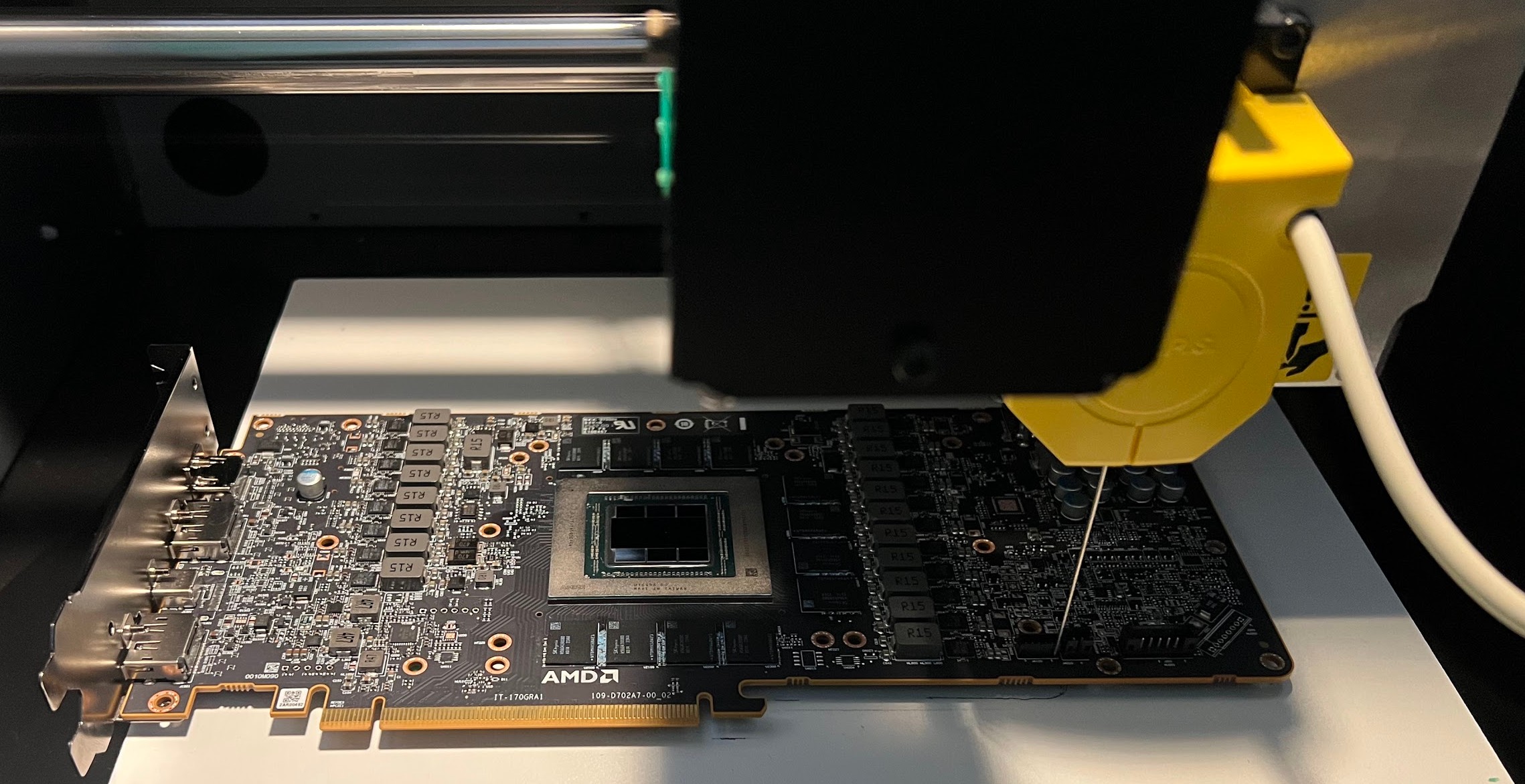
Today’s article is unfortunately based on only one card (RX 7900 XT Reference) from my own inventory, which showed a slightly higher hotspot (up to 45 Kelvin in the vertical and 38 Kelvin as delta in the horizontal setup) than the rest of the tested cards (there up to 19 Kelvin as delta in Furmark). This would certainly have been even higher with an XTX, but I only wanted to test a card that I had also disassembled (and documented) myself first beforehand. I rejected offers to analyze other affected maps as well, and not only because of time constraints. Unfortunately, all specimens had already been fundamentally “tinkered with” by the buyers, i.e. they had already been disassembled and provided with new thermal paste. However, it is no longer possible to work with this in a meaningful and plausible way.
Unfortunately, it is also a fact that replacing the used thermal paste (phase changer) in the cases known to me may only provide little remedy (namely if the rest of the conditions are not right), but in other cases on the Internet it allegedly does. This, in turn, led me to take a closer look at the heatsink and, by extension, the vapor chamber. One of the reasons why I haven’t written anything on the subject so far was, of course, the necessary time off that I allowed my family and myself over the holidays after a year. Of course, I do not claim general validity with this article, since it is only an exemplary test. However, the result shows very well that the chosen construction and a rather poor workmanship can lead to exactly this hotspot problem in individual cases, and you can definitely draw the appropriate conclusions.
Acquisition of board and cooler data
But that doesn’t mean I didn’t do anything at all. Or better: I had something done. For example, the boards and coolers captured in my 3D scanner, which has taken me a whopping 12 days in total so far, because I scanned at the highest possible resolution this time. In the meantime, you can even take a long weekend off. Until the next change in the 3D scanner. The hotspot problem was not new to me, and I started taking measurements before the wave swept through the networks. Nevertheless, unfortunately, I have only just finished.

The image above shows something that I have even observed in several cases (but more or less pronounced), because I document every card I disassemble very carefully with images during the whole process. Strictly speaking, you can already gather two interesting pieces of information from the photo. The first is the use of a so-called phase changer, i.e. a special material instead of a more or less viscous paste. This can be recognized by the formation of small air bubbles and, of course, by the very hard consistency, shiny surface and color. Second, it’s the imprints themselves that suggest very poor gap dimensions, but I’ll get to that. The fact is that you actually only take such pads if you are quite aware of the surface problems.
Since I have experimented a lot with such materials myself, I naturally have some experience with them. These materials are very easy to apply, analogous to a thin pad, but they require a so-called burn-in. With the pads I prefer (Boyd), this already takes place from approx. 52 °C and, to be on the safe side, you can also increase this up to 60 °C. This is because the material becomes fluid and then irreversibly hardens when it cools down. The thermal conductivity is comparatively low, i.e. worse than that of good pastes. Only AMD knows why they did not use the previously used, much better black graphite pads. And there’s a certain error factor that you have to take into account as well. Especially when we will look at the detail scans on the next page.

And now let’s compare the two images, please. The impression is almost identical in both pictures! If you look carefully here, you will also be able to guess what I later measured in the individual height planes, even without a 3D scan. However, I want to emphasize that here again: it only explains possible, mechanically caused problems, not potentially existing electrical ones! And so it may well be that one or the other factor here could also coincide unhappily with the problems we have highlighted.
I also noticed that the affected card (but not all) performed slightly better when installed vertically, and changing the thermal paste to a very good “normal” paste barely changed the delta, despite lower temperatures overall. The hotspot thus remained similarly pronounced, just differently and no longer quite as high as an absolute value. Reducing the TBP also brought only limited relief and the delta remained approximately the same even then.
The task was to combine the cooler of an inconspicuous card with the circuit board of the affected card! Why hasn’t anyone tested this yet? Even if it can be a purely exemplary statement due to the availability of only one card with a hotspot problem: the problem only occurred with the cooler of the originally affected card in the crossover test! That is, the hotspot was purely cooler-dependent in my case. Since PCBs deform more or less irreversibly after several heating and cooling phases and this “imprint” is in fact preserved for eternity, I first scanned the entire PCB completely (which takes about 5 days, since I’m not Croesus and can’t rely on faster laser technology).
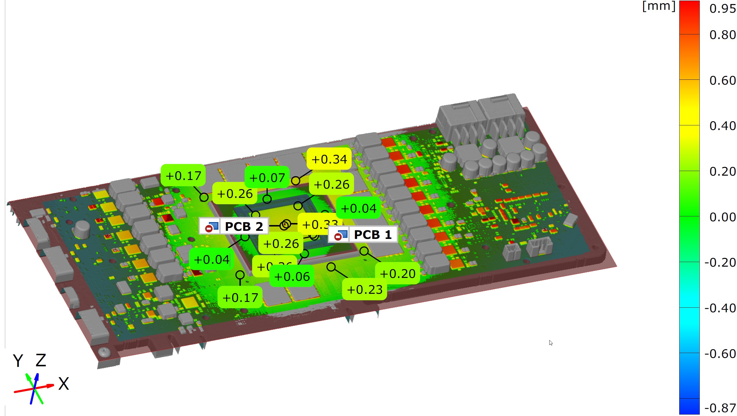
However, what can already be seen very well on a scan with a less high resolution in the horizontal plane (the vertical resolution is always maximum): We can see that the board has clearly warped around the GPU area. Of course, these are not really catastrophic values yet, but it is definitely worth a closer examination, because there must be reasons for this. Exactly this I would also not like to withhold from you. so please turn the page once.
